Purdue researchers break petaflop barrier with study of electrons in computer chips
A team led by Gerhard Klimeck of Purdue University has broken the petascale barrier while addressing a relatively old problem in the very young field of computer chip design.
Using Oak Ridge National Laboratory’s Jaguar supercomputer, Klimeck and Purdue colleague Mathieu Luisier reached more than a thousand trillion calculations a second (1 petaflop) modeling the journey of electrons as they travel through electronic devices at the smallest possible scale. Klimeck, leader of Purdue’s Nanoelectronic Modeling Group, and Luisier, a member of the university’s research faculty, used more than 220,000 of Jaguar’s 224,000 processing cores to reach 1.03 petaflops.
The team is working to help manufacturers transcend Moore’s Law, which since 1965 has anticipated the astonishing pace of technology advances. It was in that year that Intel cofounder Gordon Moore suggested in Electronics magazine that the density of transistors on a computer chip—and, therefore, the speed of that chip—would double about every 2 years. And indeed they have, with Moore’s company just this year releasing chips that hold more than 2 billion transistors on a piece of silicon just over an inch square.
An unavoidable reality
But technology makers are running across an unavoidable physical reality: There is, in fact, a limit to how many transistors you can fit onto a sliver of silicon. Within the next few years transistors will be as small as they can get.
“We’re at the stage where these transistors—the on-off switches—in these chips are as small as 20 to 30 nanometers in some of their critical widths,” noted Klimeck. “That’s along the lines of 100 to 150 atoms. We’re beginning to reach a limit where making it another factor of two smaller is going to be more and more difficult.”
Twenty nanometers is indeed very small. By comparison the shortest wavelength of visible light—belonging to violet—is 20 times wider at 400 nanometers. An especially fine strand of hair is 1,000 times wider at 20 micrometers.
The power of Jaguar has given Klimeck and Luisier the ability to pursue this task with unprecedented realism.
“What we do is build models that try to represent how electrons move through transistor structures,” Klimeck explained. “Can we come up with geometries on materials or on combinations of materials—or physical effects at the nanometer scale—that might be different than on a traditional device, and can we use them to make a transistor that is less power hungry or doesn’t generate as much heat or runs faster?
“You’re reaching the stage where you can’t think of your material being like a continuum. We experience that this material is not continuous, but discrete. And the placement of these atoms is important.”

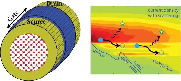
At left, schematic view of a nanowire transistor with an atomistic resolution of the semiconductor channel. At right, illustration of electron-phonon scattering in nanowire transistor. The current as function of position (horizontal) and energy (vertical) is plotted. Electrons (filled blue circle) lose energy by emitting phonons or crystal vibrations (green stars) as they move from the source to the drain of the transistor.
NEMO and OMEN
The team is pursuing this work on Jaguar with two applications, known as Nanoelectric Modeling (NEMO) 3D and OMEN (a more recent effort whose name is an anagram of NEMO).
NEMO 3D is an evolution of the earlier NEMO 1D, which was developed at Texas Instruments in the mid-1990s to model resonant tunneling diodes—devices that used the quantum mechanical ability of electrons to tunnel through a tiny barrier and appear on the other side. NEMO 3D expanded the application to three dimensions and million-atom systems, but at a cost: The systems were static, with no electron flow.
“We were able to say where the electrons would be sitting in this geometry, but we couldn’t afford computationally to model electrons injected at one end and pulled out at the other end, which we did do in NEMO 1D but in a one-dimensional space or representation.
“Around 2004 compute powers became strong enough on massively parallel machines that we could dream of combining the NEMO 1D and NEMO 3D capabilities and actually represent the device in three dimensions one atom at a time and actually inject electrons at one end and pull them out at the other end,” said Klimeck. “Having machines like Jaguar made these calculations possible. The theory of how to do that was understood with NEMO 1D, but it was computationally prohibitively expensive. OMEN is the next-generation prototype that runs on Jaguar now.”
These applications combine techniques to get the greatest possible scientific discovery out of modern supercomputers. They calculate the most important particles in the system—valence electrons located on atoms’ outermost shells—from their fundamental properties. These are the electrons that flow in and out of the system. On the other hand, the applications approximate the behavior of less critical particles—the atomic nuclei and electrons on the inner shells. The applications solve the venerable Schrödinger equation, which describes the quantum mechanical properties of a system, although Klimeck’s team has modified the equation to allow for electrons moving into and out of the system. Using OMEN Luisier has been able to model about 140,000 atoms. Without taking into account the flow of electrons, NEMO 3D is typically used to simulate 5 million to 10 million atoms.
At this scale the quantum mechanical oddities of electrons—such as the tunneling behavior studied in NEMO 1D—become increasingly important.
“Our understanding of electron flow in these structures is different,” Klimeck explained. “As you make things very small, you expose the quantum mechanical nature of the electrons. They can go around corners. They can tunnel. They can do all kinds of crazy stuff. So electrons are quantum mechanical particles at that scale, and the atoms are discrete.”
Bringing insights to the real world
The team is working with two experimental groups to bring this research to the real world. One is led by Jesus Del Alamo at the Massachusetts Institute of Technology, the other by Alan Seabaugh at Notre Dame.
With Del Alamo’s group the team is looking at making the electrons move through a semiconductor faster by building it from a material called indium arsenide rather than silicon.
“If they can move faster, maybe they will be less likely to cause losses, and you can operate them at a higher speed,” Klimeck noted. “It’s basically an on-off switch based on high-electron-mobility materials. If you have low mobility, you’re losing your energy to something else.”
With Seabaugh’s group the modeling team is working on band-to-band-tunneling transistors. These transistors bear some promise in lower-voltage operation, which could dramatically reduce the energy consumption in traditional field-effect transistors.
While there may be limited opportunities to decrease the size of a transistor, there are plenty to make devices smaller and more efficient. One problem that has not been overcome is the energy lost as heat, which leads to challenges in both powering devices and cooling them.
“Atoms like to vibrate in certain ways,” Klimeck explained, “and the vibrations are losses that come out of the device as heat. If we understand how the electrons interact with the crystal at the nanometer scale, how heat is being generated, maybe we can avoid the heat and make the transistors less power hungry. On the flip side we may be able to improve devices that convert thermal energy into electricity.”
As he notes, minimizing the power requirements and heat generation of electronics as well as harvesting energy are critically important as our lives become more and more automated.
“This is important anyplace where you don’t want to lug 40 pounds of batteries with you, for instance, if you’d like your iPhone to be lighter and run all kinds of image processing on it,” he said. “This is true for any mobile or computing technology—anything where you don’t want to waste energy, which these days is anywhere.”—by Leo Williams


