Using the Summit supercomputer at the US Department of Energy’s (DOE’s) Oak Ridge National Laboratory (ORNL), researchers at Lawrence Berkeley National Laboratory (Berkeley Lab) have confirmed and explained the results of an experiment to synthesize a new crystalline material that may hold promising applications.
Composed of alternating atomic layers of halide perovskites and non-perovskites, this new class of materials exhibits photoexcitations unique to this combined heterostructure—completely different from each layer on its own. This composite excited state could lead to future uses for the crystalline stack in next-generation solar cells, battery components, or LED devices. The team’s findings were published last year in Nature.
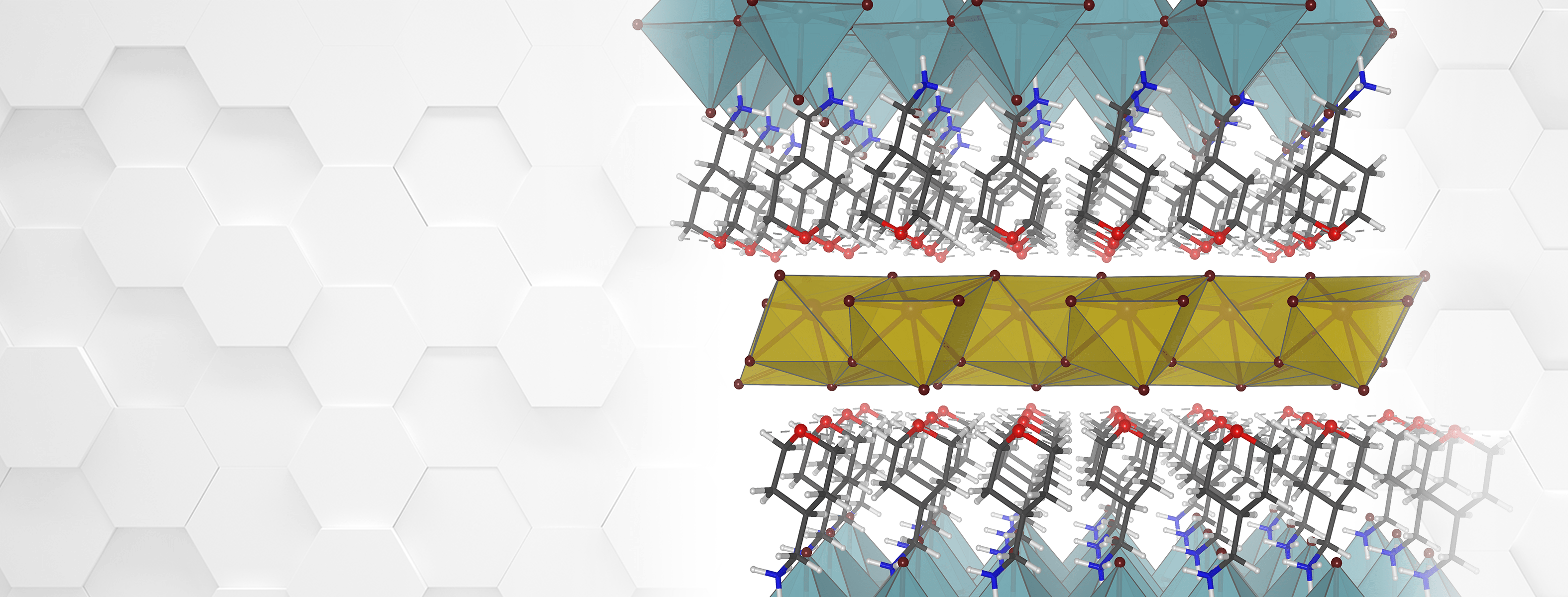
Composed of alternating atomic layers of halide perovskites and non-perovskites, this new class of materials exhibits photoexcitations unique to this combined heterostructure. This figure shows the intergrowth hetero-structure in which the perovskite and non-perovskite layers are not connected through chemical bonds. Image courtesy Marina Filip and Berkeley Lab.
“No one had made this perovskite–non-perovskite heterostructure before, and the central discovery reported in the paper is a beautiful recipe for synthesizing this heterostructure, which is—relatively speaking—cheap and easy, based on self-assembly in an aqueous solution,” said Jeffrey Neaton, associate laboratory director for energy sciences and faculty senior scientist at Berkeley Lab, as well as professor of physics at the University of California, Berkeley. Neaton worked with Marina Filip, formerly a postdoctoral fellow with Neaton and now an associate professor of physics at the University of Oxford, to perform the calculations and analysis in this study.
The new material and its method of organic synthesis were designed by Hemamala Karunadasa, an associate professor of chemistry at Stanford University and the team’s principal investigator, who leads a broad-based research program to discover and synthesize new materials with applications in clean energy.
Halide perovskites are a highly tunable class of complex semiconductors that absorb light in the visible spectrum and are cheap to synthesize. Over the past decade, halide perovskite solar cell devices have reached efficiencies above 25 percent, thereby rivaling standard silicon-based devices. However, these materials are lead based, which has raised toxicity concerns, and they are susceptible to rapid degradation. Consequently, many researchers have sought to develop new photoabsorbing perovskite-based materials with different structures and chemical compositions that offer useful optical and electronic properties. Karunadasa’s group is a leader in the synthesis of novel perovskite materials.
“The most interesting result of our calculations was that this new class of layered materials has novel optical properties, possessing photoexcitations unique to the heterostructure and completely different from what one can observe in either constituent material,” Neaton said. “Consistent with the spectral features in the measured optical data, our calculations reveal new electronic transitions distributed across both layers that result from the coupling between the perovskite and non-perovskite layers. From the point of view of optical properties, this new class of materials is not merely the sum of its parts.”
As members of the Center for Computational Study of Excited State Phenomena in Energy Materials at Berkeley Lab, Neaton and his team are also part of an effort to develop an open-source software package, BerkeleyGW, to compute the excited-state properties of complex systems. Its unique capabilities, in tandem with Summit’s 200 petaflops (200,000 trillion calculations per second) of computing power, proved integral to the project’s success.
“Our predictive calculations would simply not have been possible without Summit,” Neaton said. “We were able to tackle this highly complex system and develop a robust understanding of the computational framework we need to study similar hetero-interfaces. We think this will significantly accelerate design and discovery of new systems of this kind in the future.”
The research team’s calculations for this project represent one of the most complex systems ever studied with BerkeleyGW—a feat enabled by the software’s ability to fully exploit the GPU-accelerated architecture of Summit, which is managed by the Oak Ridge Leadership Computing Facility, a DOE Office of Science User Facility at ORNL. Jack Deslippe, Applications Performance Group lead at the National Energy Research Scientific Computing Center at Berkeley Lab, has been optimizing the BerkeleyGW code with his team to run on high-performance computing (HPC) hardware.
“BerkeleyGW was created back in the 1980s as an experiment, but it has only been ‘HPC-ized’ in the last decade or so. Now we’re able to tackle systems of the type of complexity that we’re dealing with here, on the order of thousands of atoms,” Deslippe said. “I think BerkeleyGW was the first code in this space to really use GPUs and use the full scale of a system like Summit—it’s running on nearly all of the nodes.”
With BerkeleyGW’s advanced ab initio electronic structure approaches, Neaton thinks Karunadasa’s complex crystals can serve as a test bed for understanding how novel photoexcitations—desirable for clean energy, LEDs, or energy-efficient microelectronics applications—can emerge from chemical and structural complexity.
“Halide perovskites are chemically and structurally diverse and thus have incredible variety,” Neaton said. “It is safe to say that these new perovskite-based heterostructures will inspire many new studies, both in theory and experiment.”
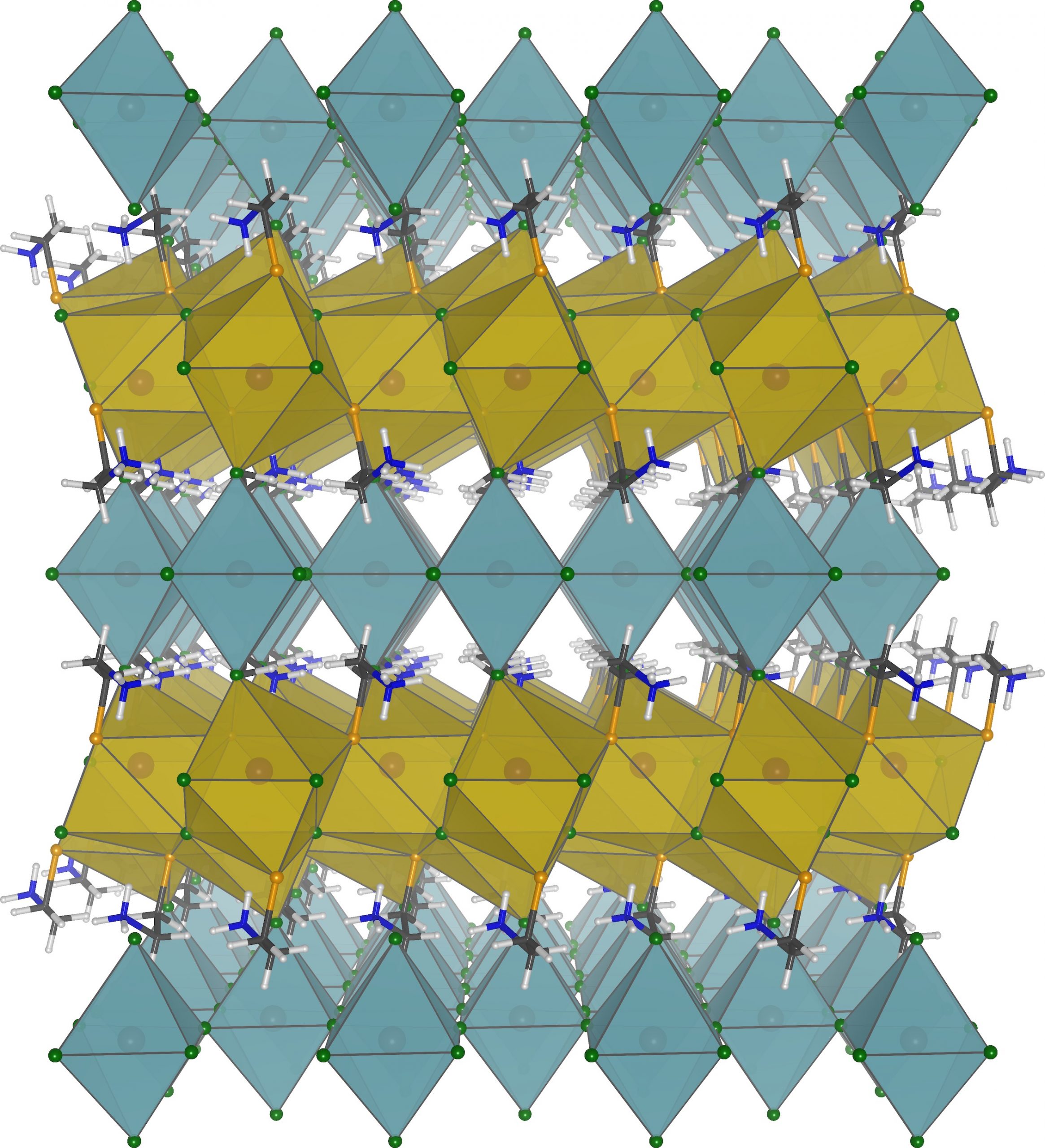
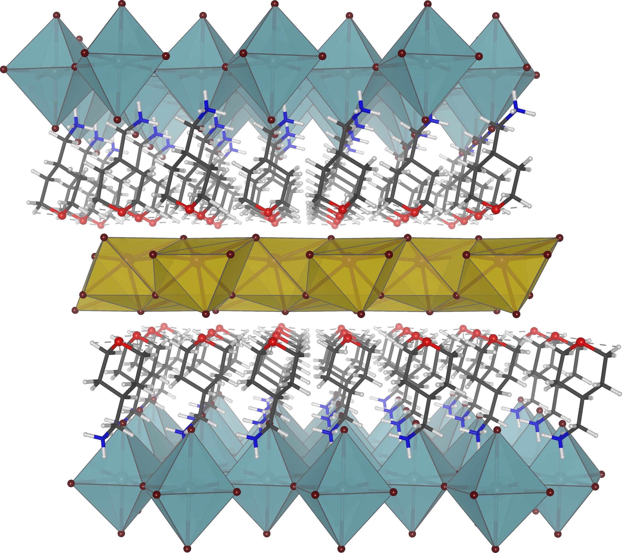
This figure of the intergrowth hetero-structure represents how the perovskite and non-perovskite layers are bound via a bridging chlorine. Image courtesy Marina Filip and Berkeley Lab.
Support for this project was provided in part by a computing allocation on Summit through the DOE Office of Science’s Innovative and Novel Computational Impact on Theory and Experiment, or INCITE, program.
Related Publication: M. L. Aubrey, A. S. Valdes, M. R. Filip, B. A. Connor, K. P. Lindquist, J. B. Neaton, and H. I. Karunadasa, “Directed assembly of layered perovskite heterostructures as single crystals,” Nature 597 (September 2021): 355–359, https://doi.org/10.1038/s41586-021-03810-x.
UT-Battelle LLC manages ORNL for DOE’s Office of Science, the single largest supporter of basic research in the physical sciences in the United States. DOE’s Office of Science is working to address some of the most pressing challenges of our time. For more information, visit https://energy.gov/science.