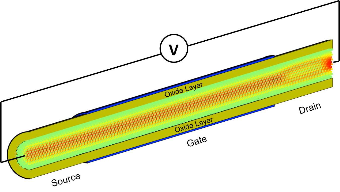
Electron current trajectories through a Si nanowire transistors composed of 55488 atoms. To facilitate the visualization, some atoms in the interior of the nanowire have been removed. Animation by Jean M. Favre, Swiss National Supercomputing Centre
Team greatly improves system size and time-to-solution for nanoelectronics models
Researchers at ETH Zurich are using America’s fastest supercomputer to make huge gains in understanding the smallest electronic devices.
The team, led by Mathieu Luisier, focuses on further developing the front line of electronics research—simulating and better understanding nanoscale components such as transistors or battery electrodes whose active regions can be on the order of 1 billionth of a meter, or about as long as your fingernails grow in one second.
Though the scales of the investigated objects are small, the team has made big progress toward more efficient computational codes. Its research was selected as a finalist for this year’s Association of Computing Machinery’s Gordon Bell Prize, one of the most prestigious awards in supercomputing.

Spatial distribution of the electron current flowing through a silicon gate-all-around nanowire field-effect transistor composed of 55,488 atoms. A voltage (V) is applied to the structure. Half of the oxide-capping layer is removed to shed light on the interior of the transistor where the atoms are colored according to the current they carry: green means no current, whereas red indicates a high concentration.
The team’s award submission is a result of research conducted on the Oak Ridge Leadership Computing Facility’s (OLCF’s) Cray XK7 Titan supercomputer. The OLCF is a US Department of Energy (DOE) Office of Science User Facility located at Oak Ridge National Laboratory.
Laptops, cell phones, and other electronic devices are becoming cheaper and more accessible while also becoming increasingly sophisticated. These advancements are largely because of the ever-shrinking dimensions of their electronic components.
However, developing next-generation hardware now requires scientists and engineers to understand material interactions at extremely small time- and size scales, leading researchers to augment experiment with simulation.
“Our goal is to study nanoscale devices, such as nanotransistors, batteries, or a variety of other new devices such as computer memories, optical switches, or light emitting diodes, on an atomic level,” Luisier said. “If you want to make these simulations accurate and truly predictive, you need to use so-called ab initio, or from first principles, simulation methods.”
Essentially, ab initio simulations allow researchers to model any atomic system from scratch, without the need for pre-calibrated material parameters. Of course, reaching such a level of accuracy is not free. The price is a thousandfold increase in computational complexity compared with, for example, semiempirical approaches that use inputs from experiments to simplify the calculation.
Researchers studying nanoelectronics thus typically have to make a compromise between simulating a realistic system size (at least 10,000 atoms) and using highly accurate ab initio methods.
To this point, though, most ab initio software packages focus on the calculation of material properties such as crystal and electronic structures, lattice vibrations, or phase diagrams and do not account for the real operating conditions—under the application of external voltage, an electron current starts to flow through active nanostructures. These transport phenomena are computationally very demanding and require a dedicated modeling approach.
Luisier and his team therefore developed a method for doing ab initio transport simulations that are large enough to investigate nanostructures with sizes relevant to industry and experimental groups. They just needed the right machine to test it.
Two partner codes, one objective
Today’s integrated circuits are composed of up to several billion transistors that are closely packed on an area that does not exceed a couple of square centimeters. With nanoelectronics, one could fit thousands of the currently manufactured nanotransistors in the width of a human hair. These systems are so small that researchers must resort to quantum theory to understand their properties.
The team uses two different software packages to accomplish this task. The community code CP2K, developed and maintained by ETH Zurich professor Joost VandeVondele, provides the ab initio description of nanostructures, whereas the OMEN code from Luisier’s group performs the quantum transport simulations based on CP2K’s inputs. By combining CP2K and OMEN, the team can get a unique “material + device” perspective of atomic systems.
Luisier explained that there are two main challenges for simulating transport through nanoelectronic components. First, researchers must calculate what they call open boundary conditions that couple the simulation with its surrounding environment and enable current flows. As a second step, they must incorporate the created boundary blocks into the Hamiltonian, a matrix that contains all of the interatomic interactions characterizing the device, and finally they must solve the resulting sparse linear system of equations. Using this approach, typical state-of-the-art simulations within the field can accurately model around 1,000 atoms.
With the emergence of hybrid supercomputers, the team realized that they needed a new simulation approach capable of leveraging the potential of CPUs and GPU accelerators. Keeping this idea in mind, two PhD students in Luisier’s group, Sascha Bruck and Mauro Calderara, implemented an original scheme allowing the team to simultaneously compute the open boundary conditions on the CPUs and create the appropriate Hamiltonian matrix on the GPUs before a short post-processing phase, then combine both results. This tour de force not only helped offload work to the GPUs but also attacked the problem on two fronts at the same time, significantly reducing simulation time.
“What allowed us to get so much faster and treat really large device structures is that we found a way to efficiently perform most of the work, solving the linear system, on Titan’s compute nodes, using extremely fast GPUs, while still keeping the CPUs busy with computing the boundary conditions at the same time,” Luisier said.
The team first tested its method on the Swiss National Supercomputing Centre’s Piz Daint machine, growing the simulation from 1,000 atoms to 15,000. For Luisier, this was extremely encouraging, but he believed the team could do more.
After these initial and successful runs, the team received time on Titan as part of the Director’s Discretionary program. Moving from Piz Daint, with its 5,000+ compute nodes, to Titan—with upwards of 18,000 nodes—allowed the team to perform a simulation with 50,000 atoms, easily beating the prior benchmark. Luisier also noted that getting to a 50,000-atom simulation did not even use all of Titan’s supercomputing power, meaning that larger simulations are not just theoretical, but likely, in the near future.
By finding a method to do ab initio quantum transport calculations on such a large system, the team is the first to run simulations that can correspond with experiments in the field, potentially helping advance research and development for next-generation electronic devices.
“If you just have 1,000 atoms, you can’t really simulate a real device,” Luisier said. “That would require simulating about 10 times as many of them. With the new method, we can really model something that looks like a transistor or a storage unit at the ab initio level. And the nanowires that we’ve been investigating have already been fabricated around 10 years ago when experimentalists were not as advanced in producing small structures as they are now. So the maximum of what we can now simulate goes beyond the smallest structures people can actually manufacture in the lab today.”
Though the codes’ sustained performance is impressive—15 petaflops, or 15 quadrillion calculations per second—Luisier emphasized that these simulations were not performed to set new computational performance benchmarks in the field, but rather were to further research.
“This is really a production code, a code that is used on a day-to-day basis,” Luisier said. “What comes out of these runs is not just FLOPS on a computer—these results are used in collaboration with experimentalists at ETH Zürich and abroad. There are a couple of groups very interested in the results because they can explain what these groups observe in their experimental devices—not only in nanotransistors but also in light-emitting components or quantum dot solar cells, to cite just a few examples.”
Oak Ridge National Laboratory is supported by the US Department of Energy’s Office of Science. The single largest supporter of basic research in the physical sciences in the United States, the Office of Science is working to address some of the most pressing challenges of our time. For more information, please visit science.energy.gov.


